Cadence and Samsung Foundry Accelerate Chip Innovation for Advanced AI and 3D-IC Applications
12 Juin 2024 - 4:45PM
Business Wire
Highlights:
- Cadence.AI digital and analog tools optimized for advanced node
SF2 gate-all-around (GAA), driving enhanced quality of results and
accelerating circuit process node migration
- Cadence’s best-in-class 3D-IC technology enabled for all of
Samsung Foundry’s multi-die integration offerings, accelerating the
design and assembly of stacked chiplets
- Cadence’s broad IP portfolio and tools for next-generation AI
designs will enable customers to achieve first-pass silicon success
and accelerate time to market
Cadence Design Systems, Inc. (Nasdaq: CDNS) today announced a
broad collaboration with Samsung Foundry that includes technology
advancements to accelerate design for AI and 3D-IC semiconductors,
including on Samsung Foundry’s most advanced gate-all-around (GAA)
nodes. The ongoing collaboration between Cadence and Samsung
significantly advances system and semiconductor development for the
industry’s most demanding applications, including AI, automotive,
aerospace, hyperscale computing and mobile.
Through this close collaboration, Cadence and Samsung have
demonstrated the following:
- Cadence.AI enables lower leakage power and
development of SF2 GAA test chips: Cadence, in close
collaboration with Samsung Foundry, has leveraged the Cadence®
Cerebrus Intelligent Chip Explorer and its AI technology in both
DTCO and implementation to minimize leakage power on their SF2 GAA
platform. Compared to the best-performing baseline flow, the
Cadence.AI result achieved a more than 10% reduction in leakage
power. As part of this ongoing collaboration, a mutual customer is
actively involved in the development of a test chip using
Cadence.AI for an SF2 design.
- Cadence backside implementation flow certified for Samsung
Foundry SF2: As a result of extensive collaboration between
Cadence and Samsung Foundry, a complete Cadence backside
implementation flow has been certified for the SF2 node to
accelerate the development of advanced designs. The full Cadence
RTL-to-GDS flow, including the Genus™ Synthesis Solution, Innovus™
Implementation System, Quantus™ Extraction Solution, Pegasus™
Verification System, Voltus™ IC Power Integrity Solution and
Tempus™ Timing Signoff Solution has been enhanced to support
backside implementation requirements such as backside routing, nano
TSV insertion, placement and optimization, signoff parasitic
extraction, timing and IR analysis, and DRC. The Cadence backside
implementation flow has been validated with a successful Samsung
SF2 test chip, demonstrating the flow is ready for use.
- Cadence has collaborated with Samsung Foundry to enable
solutions for Samsung Foundry’s multi-die offerings: The
Cadence Integrity™ 3D-IC platform is enabled for all of Samsung’s
multi-die integration offerings, and its early analysis and package
awareness features are now compliant with Samsung’s 3DCODE 2.0
version. In addition, Cadence and Samsung have expanded the
multi-die collaboration by enabling differentiating technologies
like thermal warpage analysis using the Cadence Celsius Studio and
system-level LVS with Cadence Pegasus Verification System. Cadence
is also supporting Samsung with a package PDK that reduces design
time with the Allegro X system. Combined with the Integrity 3D-IC
platform, it optimizes the package design flow.
- Cadence.AI’s Virtuoso Studio flow successfully deployed for
analog circuit process migration: Purpose-based instance
mapping in the AI-powered Virtuoso Studio provided rapid
retargeting of the schematics, while circuit optimization in
Virtuoso Studio’s Advanced Optimization Platform helped Samsung
achieve a 10X improvement in turnaround time when migrating a
100MHz oscillator design from 14nm to 8nm. In addition, a
FinFET-to-GAA analog design migration reference flow is available
for joint customers, with successful experimental results.
- Cadence mmWave RFIC design flow successfully used to tapeout
14RF circuit design: Cadence and Samsung successfully taped out
a 48GHz power amplifier design, representing silicon validation of
the robust, full system reference flow that leverages the Cadence
EMX Designer to create passive devices with fast modeling and
layout automation. Full design EM extraction with the EMX 3D Planar
Solver and EM/IR analysis using Voltus XFi and Quantus ensured that
the IC met aggressive metrics, Pegasus was used for signoff
DRC/LVS, while AWR VSS provided a seamless environment to carry out
initial system-level budgeting and post-layout verification. Mutual
customers can feel confident utilizing this flow to deliver
leading-edge designs to market in a timely manner.
- Cadence Pegasus Verification System is certified for
Samsung Foundry's 4nm and 3nm process technologies: Through the
collaboration with Samsung Foundry, the Cadence physical
verification flow is optimized to allow mutual customers using
Samsung Foundry’s advanced nodes to reach signoff accuracy and
runtime goals for a faster time to market. The Pegasus system is
now certified across multiple advanced nodes at Samsung Foundry,
which are proven and in production by customers, with simplified,
all-inclusive licensing support. The Pegasus system is integrated
into the AI-powered Cadence Virtuoso Studio as iPegasus to enable
in-design signoff quality DRC and interactive metal fill in the
layout implementation, offering up to 4X faster turnaround
times.
- Cadence IP portfolio offers comprehensive industry
solutions on advanced Samsung nodes:
- Cadence’s latest IP built on Samsung SF5A includes
industry-leading PHY IP for 112G-ULR SerDes, PCIe® 6.0/5.0, UCIe™,
DDR5-8400, DDR5/4-6400 Memory and USB 2.0, offering customers
complete platform solutions
- Cadence’s PHY IP for PCIe 6.0 on Samsung SF5A has been
successfully certified for PCIe 5.0 x8 compliance and demonstrated
seamless interoperability with other PCIe 5.0/6.0 system and test
equipment, further showcasing its PCIe solution maturity
- Cadence is furthering its partnership with Samsung Foundry by
pushing the performance envelope, designing advanced memory IP for
GDDR7 on Samsung SF4X and SF2, and helping reshape the HPC/AI
industry with this new memory standard.
- Advanced verification for AI design complexity: Samsung
Foundry applied Cadence’s advanced verification technologies, such
as the Palladium Enterprise Emulation System, JasperC, STG, and
Xcelium ML, to tackle rising AI chip complexity and achieve
time-to-market requirements in SF3.
“We are honored to partner with Samsung, a true example of a
chips-to-systems company, to bring this technology for our joint
partners to design the next generation of intelligent systems,”
said Tom Beckley, senior vice president and general manager in the
Custom IC & PCB Group at Cadence. “The hyperconvergence of AI
with modern accelerated compute requires a strong silicon
infrastructure. With these new AI-powered, certified design flows
and standardized solutions, mutual customers can confidently design
for Samsung advanced nodes while achieving their design and
time-to-market goals.”
“Samsung and Cadence have a close collaboration to advance
technology and help our customers deliver competitive designs to
the market efficiently,” said Sangyun Kim, Vice President and head
of Foundry Design Technology Team at Samsung Electronics. “Our
joint efforts enable customers to utilize Samsung’s latest process
and technology innovations to push the limits for the most advanced
AI, hyperscale computing and mobile SoC designs.”
To learn more about Cadence AI offerings, please visit:
Cadence.ai.
About Cadence
Cadence is a pivotal leader in electronic systems design,
building upon more than 30 years of computational software
expertise. The company applies its underlying Intelligent System
Design strategy to deliver software, hardware and IP that turn
design concepts into reality. Cadence customers are the world’s
most innovative companies, delivering extraordinary electronic
products from chips to boards to systems for the most dynamic
market applications, including consumer, hyperscale computing, 5G
communications, automotive, mobile, aerospace, industrial and
healthcare. For 10 years in a row, Fortune magazine has named
Cadence one of the 100 Best Companies to Work For. Learn more at
cadence.com.
© 2024 Cadence Design Systems, Inc. All rights reserved
worldwide. Cadence, the Cadence logo and the other Cadence marks
found at www.cadence.com/go/trademarks are trademarks or registered
trademarks of Cadence Design Systems, Inc. All other trademarks are
the property of their respective owners.
Category: Featured
View source
version on businesswire.com: https://www.businesswire.com/news/home/20240612720853/en/
Cadence Newsroom 408-944-7039 newsroom@cadence.com
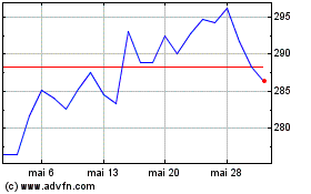
Cadence Design Systems (NASDAQ:CDNS)
Graphique Historique de l'Action
De Mai 2024 à Juin 2024

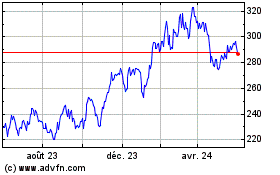
Cadence Design Systems (NASDAQ:CDNS)
Graphique Historique de l'Action
De Juin 2023 à Juin 2024
